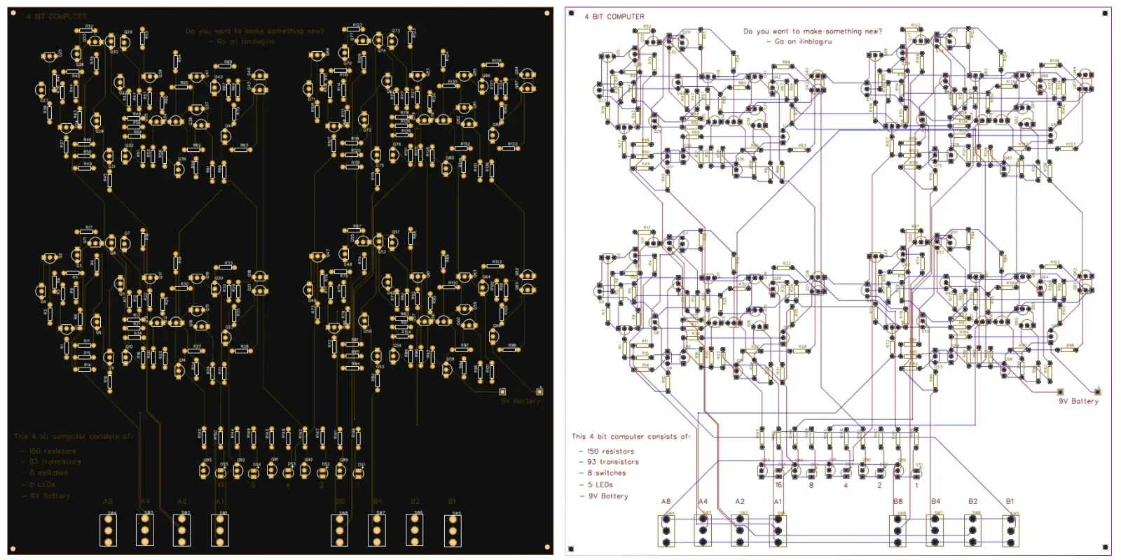
How much of a calculator can you build before it stops feeling like magic? In 2019, I decided to find out. I did not use a microcontroller, an adder chip, or software that performed the arithmetic for me. Boolean rules became transistor circuits, those circuits became a one-bit full adder, and four full adders became a large black circuit board on which the calculation was visible.
The finished machine accepts two unsigned four-bit numbers, each from 0 to 15, and displays their five-bit sum on LEDs. It is a deliberately impractical calculator. Its purpose is not speed or convenience, but understanding: every switch, current path, carry, and output remains out in the open.
The clean final board hides the most useful part of the story. My first prototype almost worked. It produced the correct sum for 1 + 0, but also raised a carry that should not have existed. I worked through solder, components, and even the direction of the transistors before finding the real culprit: a single resistor whose other end led nowhere.
Addition, one bit at a time
Binary addition follows the same column-by-column rule as decimal addition. At the smallest scale there are only four cases: 0 + 0, 0 + 1, 1 + 0, and 1 + 1. The last case produces 10 in binary—a sum bit of 0 and a carry of 1.
A full adder handles one column. It receives the two input bits, and , plus the carry from the previous column, . It produces a sum bit and a carry for the next column:
I built exclusive OR from the three elementary operations used throughout the original design—NOT, AND, and OR:
Four copies of the full adder form a ripple-carry adder. Each stage sends its carry into the next stage, just as a handwritten addition carries from one column to the next.
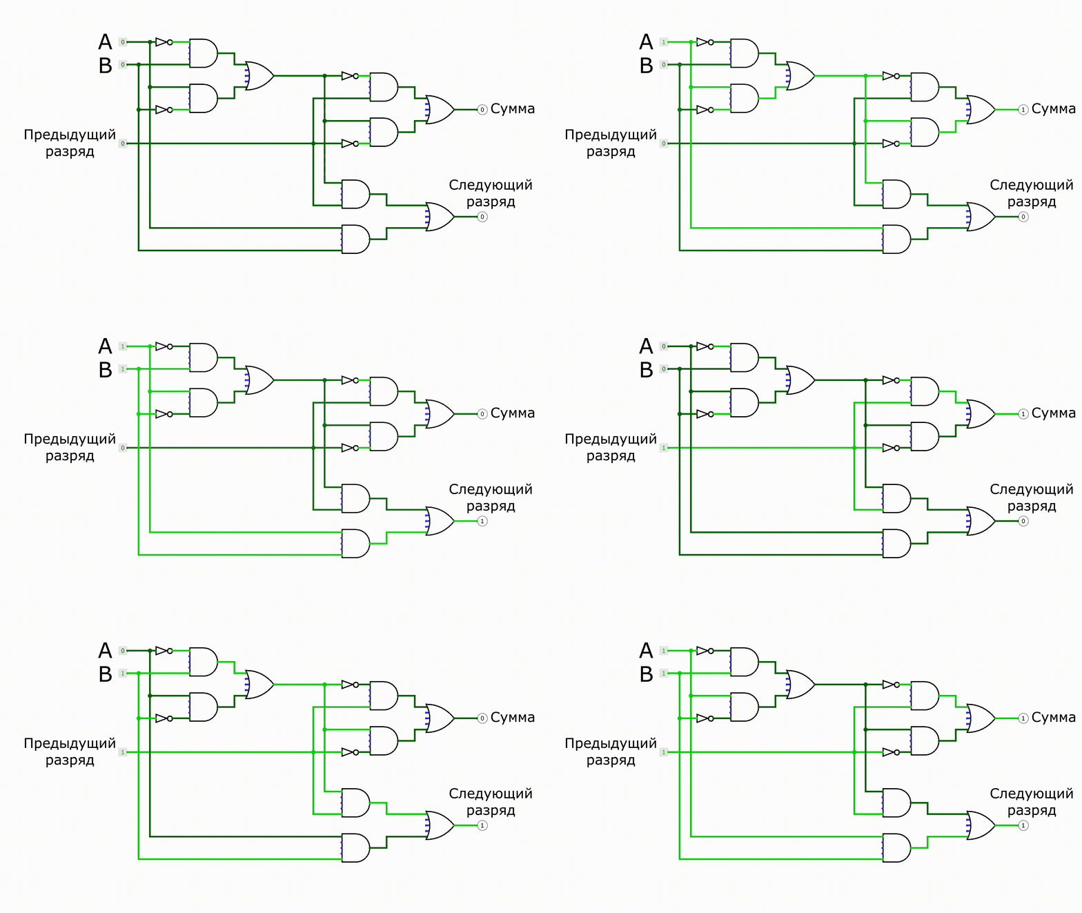
Turning logic gates into transistor circuits
Digital logic maps naturally onto voltage: a low voltage represents 0 and a high voltage represents 1. A transistor can act as a switch between those states. In the inverter used here, a high input opens a path to ground and pulls the output low; a low input closes that path and lets the output rise. Series and parallel transistor paths, together with inverters and resistors, provide the conditions needed for AND and OR.
That simple description expands quickly in a real schematic. I replaced every logic-gate symbol with a network of 2N2222A transistors and resistors, then connected those networks into one full adder. A single bit already required 22 transistors and 35 resistors.
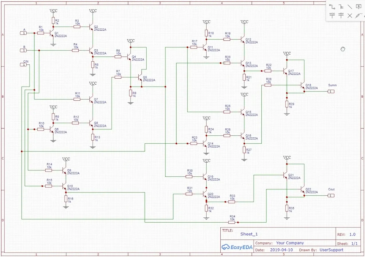
Once I became comfortable with the circuit-design software, repeated sections made the schematic surprisingly quick to draw. The PCB layout was a different kind of problem. Components had to be positioned so the copper traces stayed short and crossed as little as possible. It felt less like electronics and more like one of those puzzles where you untangle the edges of a graph—helped by tea, biscuits, and plenty of rearranging.
I considered etching the board at home with toner transfer, but I wanted a clean solder mask and silkscreen, and I did not want to turn the room into a chemistry bench. I ordered ten small green boards from a manufacturer in China instead. There was one uncomfortable detail: I had not found a reliable way to simulate the complete circuit. If the design was wrong, I would discover it only after a month of waiting.
The R16 mystery
The manufactured boards looked professional. I soldered the first one immediately and began testing. Most of the behavior looked right, but one case exposed a strange failure: with one input high and the other low, the sum output was correct while the carry output also went high. The circuit was claiming that 1 + 0 was both 1 and large enough to carry.
I called the fault R16 and entered the familiar debugging spiral. I reflowed suspicious joints and checked for accidental solder bridges. I cleaned the board in case flux residue was conducting a small current. I desoldered and tested components, burning my fingers on hot leads in the process. Conflicting transistor pinout diagrams online made me question their orientation, so I tried that too. Finally, I checked the copper traces with a multimeter. Everything I suspected appeared to be fine.
At one low point I even took the schematic to the head of Radioelectronic Physics at Novosibirsk State University. His immediate verdict was that the circuit could never work. That made the mystery feel rather final—but the verdict turned out to be wrong as well.
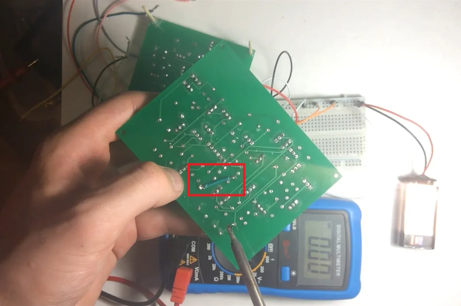
After the board had sat untouched for a couple of months, I returned to it and noticed something odd around the component that had given the bug its name. R16 looked connected on the component side, yet one of its pads had no route onward. The intended ground connection existed in the schematic, but it had never become a copper trace on the board. The resistor was floating.
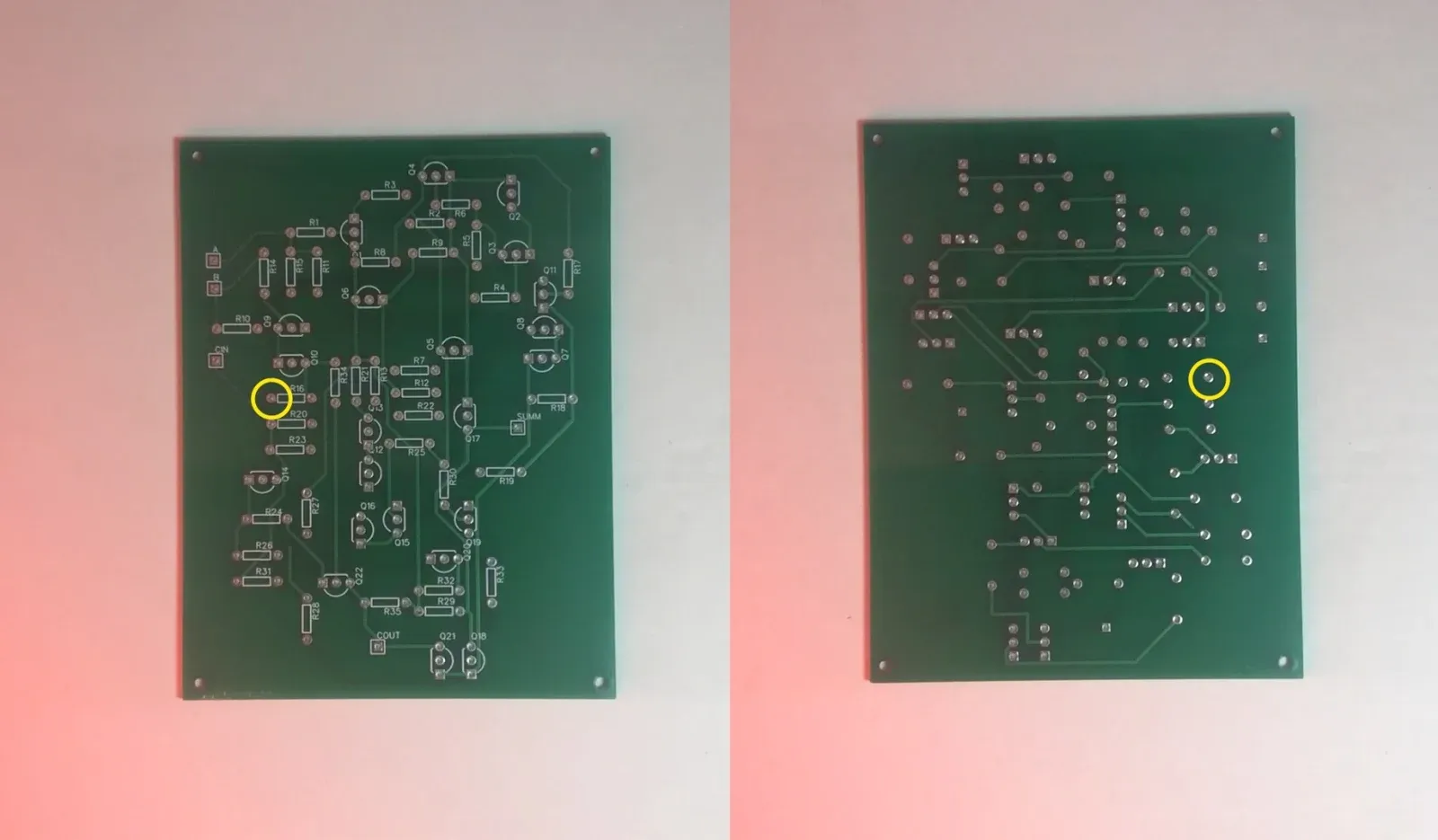
This was the best possible failure. I did not need to redesign and reorder the boards. A short jumper wire from R16 to the nearest ground point repaired the circuit in minutes—and the full adder immediately began producing the right carry.
Proving the building block
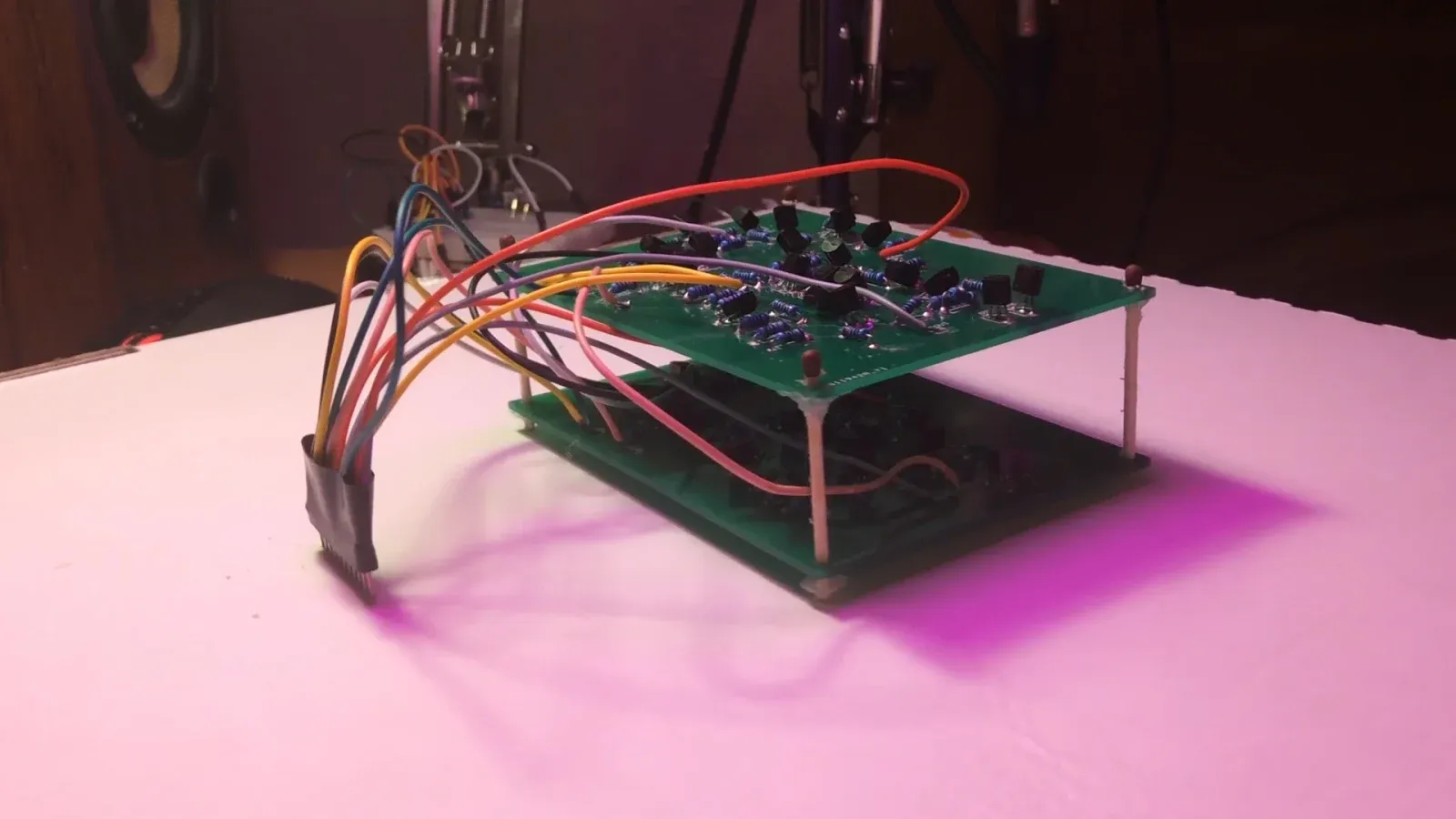
One working bit was not enough to show that carries would move correctly between stages. I stacked two corrected boards into a small two-bit “sandwich,” connected the carry-out of the first to the carry-in of the second, and built a control panel with four toggle switches and three output LEDs.
The prototype had possible input configurations. I tested every one, and every result was correct. More importantly, the experiment confirmed the central idea: a reliable full-adder cell could be repeated to build a wider machine.
From a wired stack to one four-bit board
The two-bit prototype proved the design, but it also showed why the final version needed a single PCB. I copied the full-adder cell four times, chained the carries, and integrated the controls and display. Eight switches set two four-bit inputs, with weights 1, 2, 4, and 8. Five LEDs display the result, including the final carry at weight 16.
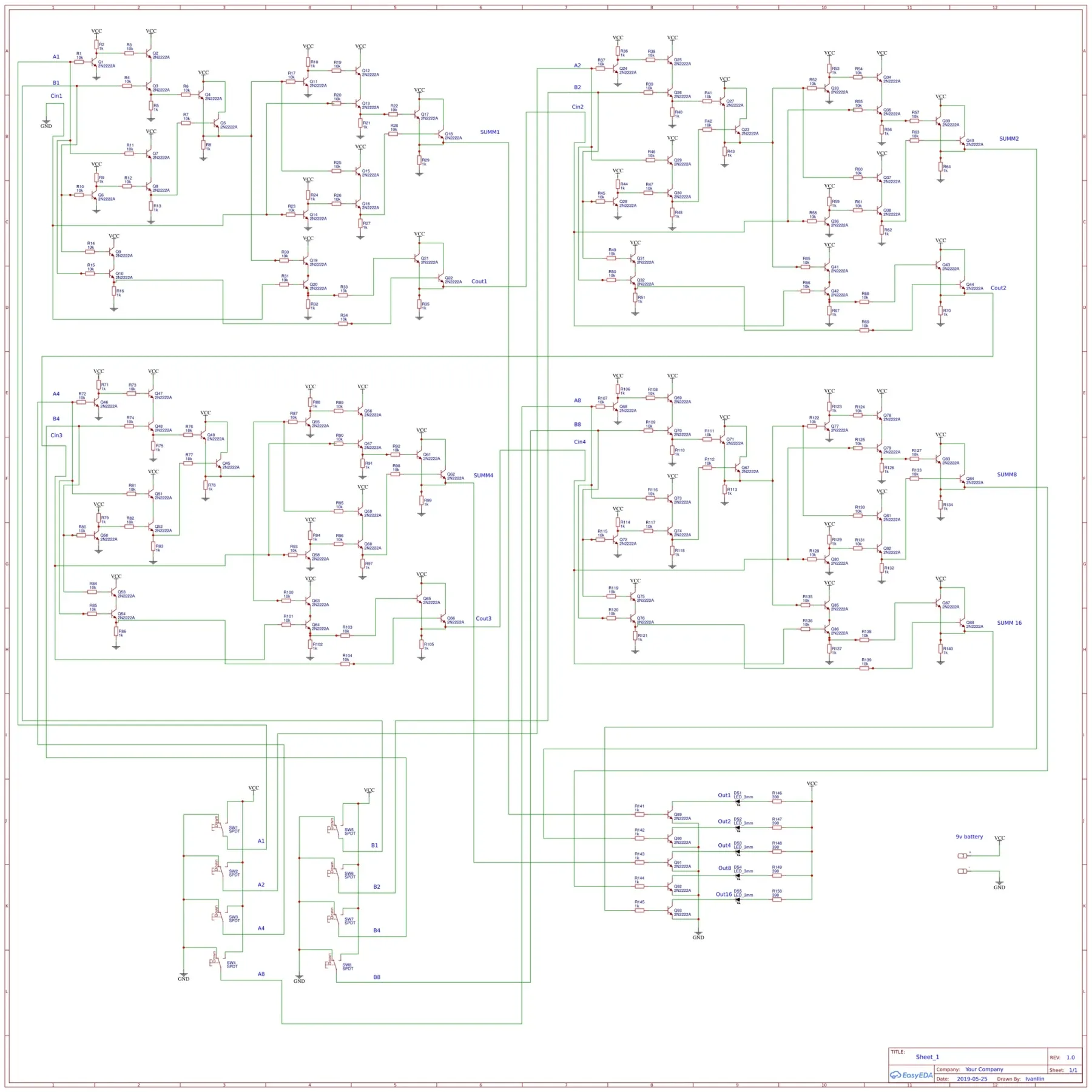
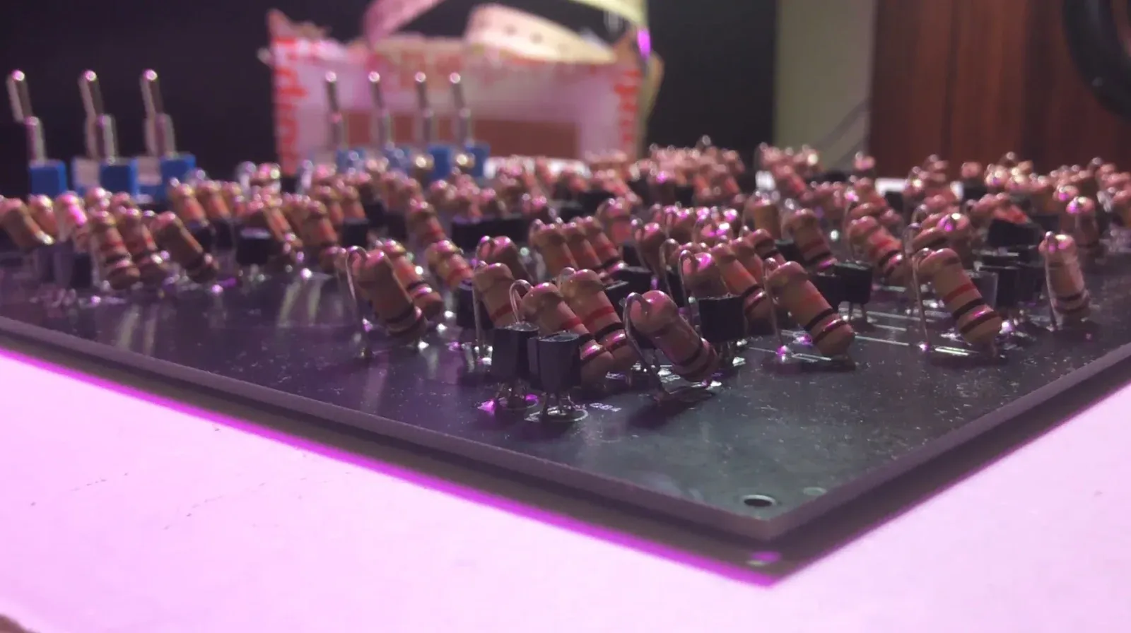
The larger board was more expensive, so I ordered five rather than ten and chose a black solder mask for the final revision. This time I checked every connection repeatedly before sending the design away. When the boards arrived, populating one took two long evenings: 150 resistors and 93 transistors, all soldered by hand, followed by eight switches, five LEDs, and the battery connection.
All 256 combinations
The final board worked on its first full test. Because the eight input switches each have two states, there are input configurations—the complete set of 16 × 16 ordered pairs. I checked every one manually, and all 256 produced the correct result.
At the upper limit, the machine computes:
or 15 + 15 = 30. The fifth LED is what makes that final carry visible.
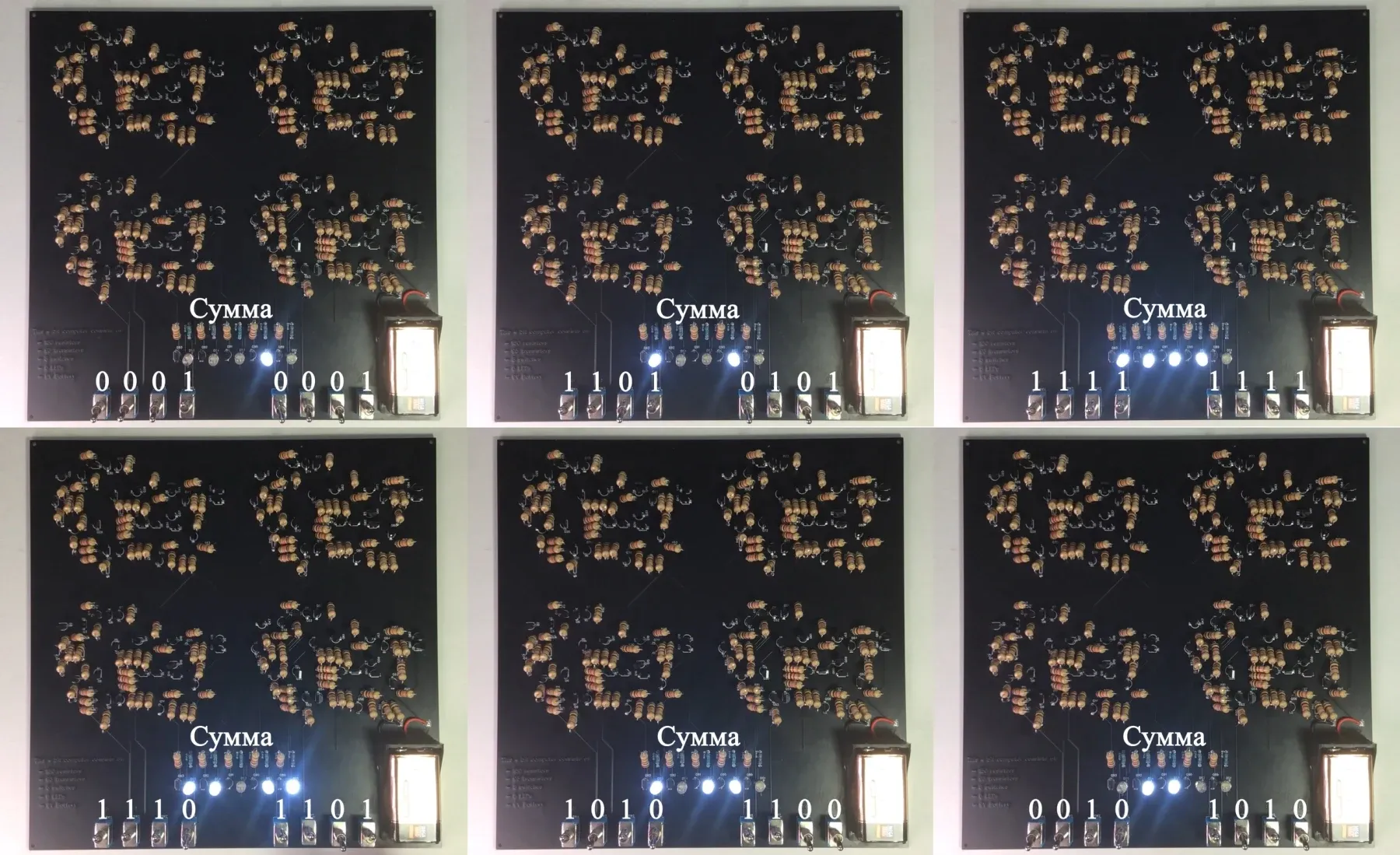
Modern hardware compresses vastly more logic into a package smaller than one of this board’s switches. This project does the opposite: it spreads one elementary operation across an entire surface so that every abstraction becomes tangible. You can follow a carry from one stage to the next, recognize the same circuit repeated four times, and watch an answer appear one LED at a time.
The most memorable lesson was just as physical. Correct Boolean algebra is not enough if one connection never reaches the copper. R16 turned a frustrating failure into the best explanation of what building hardware from first principles actually means.
My original write-ups
I originally documented this project in two Russian-language articles. This page brings my write-ups together in English, using the original diagrams, build photographs, and debugging notes from the project.